$DECLASSwnMfUvY5KfUN2LbKgyHXwmh39mGpJd7bjJw5A71pumpBuy
Declassified
Releases / Release 06 / DOW-UAP-D118
Department of War

AAWSAP DIRD, Aerospace Applications of Programmable Matter, December 2009

This is a December 2009 Defense Intelligence Reference Document prepared under AAWSAP. It surveys smart materials, quantum dots, metamaterials, dynamic windows, thermal and energy harvesting for spacecraft, and speculates about applications out to 2050. It carries no UAP incident reporting.

Record
DOW-UAP-D118
Release
Release 06 · Sep 18, 2026
Incident
2009-12-14 · Las Vegas, Nevada
Pages
20
Verdict
Partly new
Source
war.gov ↗
Context · why this verdict

A 20-page technical reference paper on programmable matter that has no overlap with earlier releases beyond a shared boilerplate title page with DOW-UAP-D120, so the content is new to the archive but is a speculative literature synthesis, not an event record.

Findings in this document

4 findings

New SIG

Report warns of hackers gaining control over programmable matter

  • Verbatim
    We must be extremely cautious about handing malicious hackers the keys to matter itself!
    DOW-UAP-D118 · Release 06 · page 10 · war.gov ↗
  • Inference · AI interpretation

    This may reflect that the authors treated cybersecurity of reconfigurable materials as a significant obstacle.

New or already public? No matching text in earlier releases per the overlap data.

New SIG

Paper cites 2003 LBNL/ASHRAE dynamic-window energy savings study

  • Verbatim
    The ASHRAE study found that across all eight climate zones, buildings with low-emissivity ("low-E") glass saved an average of 8-15 percent on their total annual energy (heating, cooling, and ventilation) costs, whereas the addition of dynamic window systems saved an additional 6-19 percent.
    DOW-UAP-D118 · Release 06 · page 11 · war.gov ↗
  • Context

    The paper uses this study to support its case for near-term smart-window applications.

New or already public? No earlier archive pages match this text.

New SIG

Document describes 2050 scenarios as partly speculative

  • Verbatim
    Many elements of the preceding scenario are based on current and emerging technologies; others are speculative.
    DOW-UAP-D118 · Release 06 · page 20 · war.gov ↗
  • Verbatim
    by 2050 it seems likely that our grandchildren will have difficulty imagining a world where these objects are made from traditional, inert materials.
    DOW-UAP-D118 · Release 06 · page 19 · war.gov ↗

New or already public? No overlap with earlier releases for these pages.

New SIG

DIRD judges smart windows most promising programmable-matter research for next 5 years

  • Verbatim
    near-term applications such as smart windows and energy-saving metapolarizers, which offer direct and immediate economic advantages (namely energy savings) and which dovetail neatly with existing infrastructure, should be considered the most promising for research over the next 5 years.
    DOW-UAP-D118 · Release 06 · page 19 · war.gov ↗
  • Context

    The DIRD is a DIA reference product dated 14 December 2009 and prepared under AAWSAP.

  • Inference · AI interpretation

    This suggests the authors ranked commercially viable applications above the more ambitious aerospace concepts discussed elsewhere in the paper.

New or already public? Only the title page overlaps with DOW-UAP-D120 (Release 06); the body text has no match in the archive.

Page by page

The pages and what the AI read on them

The transcription is the page reader's: black bars mark what the government redacted; hatched tags mark personal data we removed.

Page 1

Page 1 of 20

This is the cover page of a Defense Intelligence Reference Document titled "Aerospace Applications of Programmable Matter," dated 14 December 2009 with an ICOD of 1 December 2009 and document number DIA-08-0911-016. It is marked UNCLASSIFIED//FOR OFFICIAL USE ONLY and bears the Defense Intelligence Agency seal.

UNCLASSIFIED//FOR OFFICIAL USE ONLY Defense Intelligence Reference Document Acquisition Threat Support 14 December 2009 ICOD: 1 December 2009 DIA-08-0911-016 Aerospace Applications of Programmable Matter UNCLASSIFIED//FOR OFFICIAL USE ONLY
Page 2

Page 2 of 20

This is the title page of the report "Aerospace Applications of Programmable Matter," prepared by the Defense Intelligence Agency's Acquisition Support Division, with an administrative note on photograph copyright and contact information for questions about the AAWSA program.

UNCLASSIFIED//FOR OFFICIAL USE ONLY Aerospace Applications of Programmable Matter Prepared by: Acquisition Support Division (DWO-3) Defense Warning Office Directorate for Analysis Defense Intelligence Agency Author: AAP Person 90 Administrative Note COPYRIGHT WARNING: Further dissemination of the photographs in this publication is not authorized. This product is one in a series of advanced technology reports produced in FY 2009 under the Defense Intelligence Agency, Defense Warning Office's Advanced Aerospace Weapon System Applications (AAWSA) Program. Comments or questions pertaining to this document should be addressed to AAP Person 1, AAWSA Program Manager, Defense Intelligence Agency, ATTN: CLAR/DWO-3, Bldg 6000, Washington, DC 20340-5100. ii UNCLASSIFIED//FOR OFFICIAL USE ONLY
Page 3

Page 3 of 20

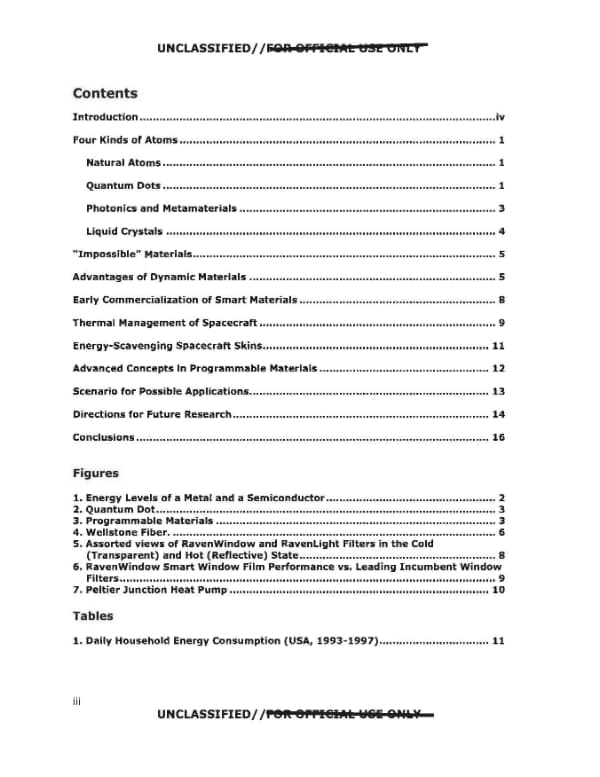
This is the table of contents page of a report on programmable and smart materials, listing its sections, figures and tables. It has no redaction marks.

UNCLASSIFIED//FOR OFFICIAL USE ONLY Contents Introduction ............................................................iv Four Kinds of Atoms .......................................................... 1 Natural Atoms ............................................................... 1 Quantum Dots ............................................................... 1 Photonics and Metamaterials .................................................. 3 Liquid Crystals ............................................................... 4 "Impossible" Materials ........................................................ 5 Advantages of Dynamic Materials ............................................... 5 Early Commercialization of Smart Materials ..................................... 8 Thermal Management of Spacecraft ............................................. 9 Energy-Scavenging Spacecraft Skins ........................................... 11 Advanced Concepts in Programmable Materials ................................. 12 Scenario for Possible Applications ............................................ 13 Directions for Future Research ................................................ 14 Conclusions ................................................................ 16 Figures 1. Energy Levels of a Metal and a Semiconductor ................................. 2 2. Quantum Dot ............................................................... 3 3. Programmable Materials ..................................................... 3 4. Wellstone Fiber ............................................................ 6 5. Assorted views of RavenWindow and RavenLight Filters in the Cold (Transparent) and Hot (Reflective) State ........................................... 8 6. RavenWindow Smart Window Film Performance vs. Leading Incumbent Window Filters ....................................................................... 9 7. Peltier Junction Heat Pump ................................................... 10 Tables 1. Daily Household Energy Consumption (USA, 1993-1997) ............................. 11 iii UNCLASSIFIED//FOR OFFICIAL USE ONLY
Page 4

Page 4 of 20

Page iv of a white paper introducing Programmable Matter smart materials and their possible aerospace applications, including satellite repair by software update and defensive capabilities such as camouflage and laser deflection. The page is marked UNCLASSIFIED//FOR OFFICIAL USE ONLY.

UNCLASSIFIED/ j FOR OFFICIAL O!JE OIILT Aerospace Applications of Programmable Matter Introduction For the owners of a $100 million satellite-a TV broadcast satellite, for example-avoiding bankruptcy often depends on the spacecraft's continued good health until its scheduled replacement is in orbit. Unfortunately, numerous failure modes are possible, including blown fuses, failed sensors, and browned-out solar arrays. The common trait of most such failures is that they cannot be repaired from the ground. In addition, it is not typically possible to repurpose a spacecraft or its components for new services that no one foresaw at the time of manufacture. Either way, a new satellite is required. However, when sensors, filters, emitters, and photovoltaic solar panels are made of Programmable Matter smart materials, the solution to a component failure or new mission requirement might be as simple as a software update. Other advantages of dynamic materials include advanced energy management and energy scavenging from a variety of sources. Smart materials can even create new defensive capabilities, such as chameleon-style camouflage, deflection of laser beams, and even outright invisibility. If it becomes possible to change the properties of certain materials on demand, based on remotely triggered instructions, the benefits for spacecraft-both crewed and autonomous-will be considerable. This white paper-by no means an exhaustive reference-is intended to serve as a primer on the principles behind smart materials and their possible aerospace applications over the next 50 years. UNCLASSIFIED//liQR Qfli1&'10L: P!iii Ctr! Y iv UNCLASSIFIED/ //FOR OFFICIAL USE ONLY
Page 5

Page 5 of 20

Page 1 of an undated unclassified (For Official Use Only) text titled "Four Kinds of Atoms", introducing natural atoms and quantum dots ("artificial atoms") and explaining semiconductors and electron shells and band gaps.

UNCLASSIFIED//FOR OFFICIAL USE ONLY Four Kinds of Atoms All matter is made of atoms and derives its properties, in part, from the fact that atoms are discrete objects yet are so small and so close together that light waves cannot "see" them individually. By extension, neither can electric and magnetic fields. To a photon, or to a large electrical current, matter appears to be made up of continuous substances rather than discrete building blocks. This fact is critically important in understanding the optical, electrical, and even thermal properties of materials. Equally important are the discoveries of recent decades, showing at least four different kinds of "atoms" that meet this same general description. NATURAL ATOMS Natural atoms are the 92 elements of the periodic table. Actually there are more, but the rest have unstable nuclei that will eventually fly apart Into smaller atoms and loose subatomic particles that can damage the materials around them. For engineering purposes, this makes them unreliable building blocks. However, 92 building blocks allow for a staggering number of combinations, and all the materials with which we are familiar-natural ones like coal and diamonds, ancient ones like bronze and glass, and modern ones like silicon carbide and gallium arsenide-are merely "Tinkertoy" sculptures of these natural atoms. QUANTUM DOTS A quantum dot is a very small grouping of tightly confined electrons whose collective behavior resembles that of a natural atom. For this reason, quantum dots are sometimes known as "artificial atoms." To describe how this trick is accomplished, it is first necessary to talk about electrons and how they behave. Most materials are either conductors, which permit the free flow of electrons, or insulators, which resist it. Semiconductors are insulators that are capable of conducting electrons above a certain threshold energy-a useful trick that makes integrated circuits and other electronics possible. The most familiar semiconductor is silicon, which is used to make the vast majority of microchips found in today's consumer and industrial electronics. Because silicon's native oxide, SiO2, is the main component of sand and rocks, it is readily available and relatively inexpensive. In addition, when melted, purified, and hardened into sheets, silicon dioxide serves as one of our familiar insulators and building materials: glass. Unlike most other semiconductors, silicon is also nontoxic. The electrical properties of a semiconductor like silicon are of course fixed by the laws of physics. Atoms hold electrons in shells that increase in size, capacity, and potential energy the farther they are from the nucleus. "Valence" electrons are found in full (or nearly full) shells, where there are few empty spaces through which electrons can move. These electrons tend to stay at home, so their levels exhibit a large electrical resistance and do not permit electricity to flow. "Conduction" electrons are found in shells that are more than half-empty and have lots of open space, enabling electrons to travel freely through them and move easily from one atom to another. Between these layers is a "band gap" of forbidden energies. Here, there exist no electrons at all-ever. UNCLASSIFIED//FOR OFFICIAL USE ONLY 1
Page 6

Page 6 of 20

This is page 2 of a Department of War AAWSAP DIRD document on programmable matter, containing a figure comparing energy levels of metals and semiconductors and explanatory text on conduction electrons, band gaps and quantum dots. The page is marked UNCLASSIFIED//FOR OFFICIAL USE ONLY and contains no redactions.

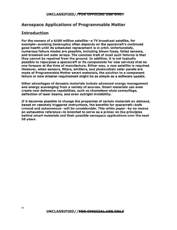
UNCLASSIFIED// FOR OFFICIAL USE ONLY Valence Band Conduction Band Conduction Band Band Gap Metal Semiconductor Figure 1. Energy Levels of a Metal and a Semiconductor. In a metal, many electrons reside in the conduction band and can be pushed to neighboring atoms with only a tiny addition of thermal or electrical energy. In a semiconductor, enough energy must first be added to excite the electron out of the valence band, across the band gap, and into the conduction band. Thus, to conduct electricity, semiconductors require much higher voltages and temperatures than do metals. Electrons below the band gap of a semiconductor behave as though they were in an insulator, while electrons above the band gap behave as though they were in a conductor. They flow easily and can be used to store or transport energy and information. The difference between a metal and an insulator is that the outermost electron shell of a metal atom is more than half-empty. It has lots of conduction electrons and lots of room for them to move around. An insulating material, such as sulfur, has an outer shell that is almost completely filled. All its electrons are valence electrons"homebodies that do not like to travel. Semiconductors have outer shells that are approximately half-filled. With the input of energy, their electrons can jump to a higher level where they find open space to travel through. Conduction electrons can also be "donated" by neighboring atoms. A "quantum dot" is simply a very small structure-usually on the order of 5-20 nanometers-that contains a modest number of conduction electrons, which it confines in all three dimensions and prevents from leaving the structure. In addition, because the Heisenberg uncertainty principle requires position uncertainty to increase when particle momentum is restricted, the trapped electrons are unable to hold a well-defined position and instead behave as standing waves that resemble the orbitals of, and exhibit many of the same properties as, a natural atom. However, there are two major differences between a quantum dot and a natural atom. First, there are far more than 92 possible configurations-an infinite number, in fact-for the confined electrons. Thus, with quantum dots it is possible to create designer atoms with properties that simply do not occur on the periodic table. If we want to, we UNCLASSIFIED//FOR OFFICIAL USE ONLY 2
Page 7

Page 7 of 20

Page 3 of a December 2009 AAWSAP report on programmable matter, describing quantum dots and programmable materials with diagrams of a quantum dot and a programmable material structure, and opening a section on photonics and metamaterials. The page body is continuous text with no redactions.

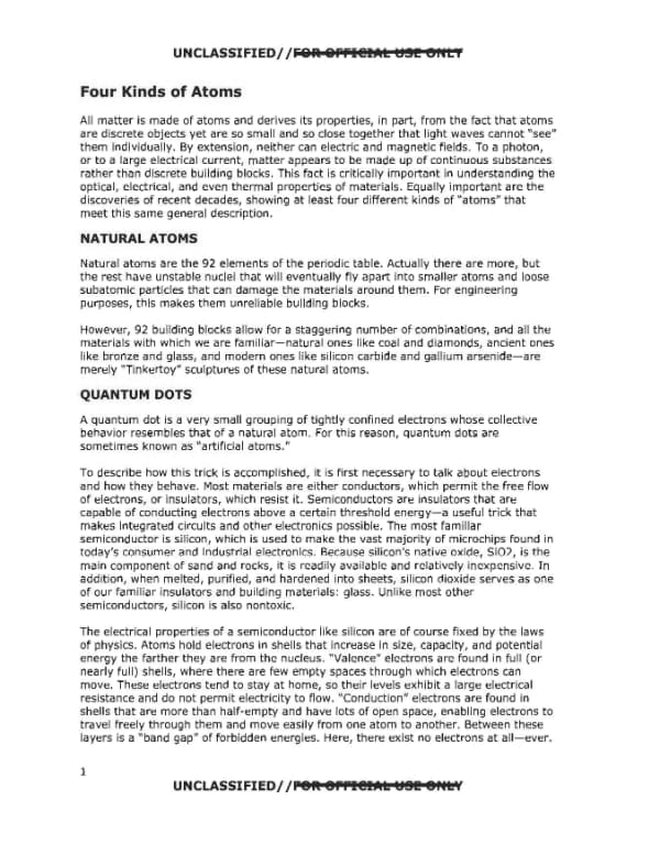
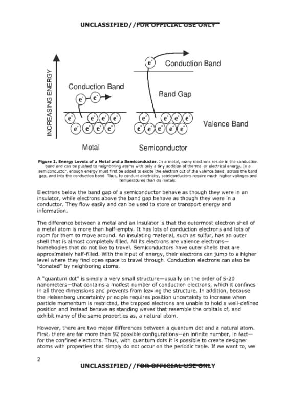
can exert precise control over their optical, electrical, thermal, and magnetic properties rather than simply selecting these properties from the limited catalog nature has provided. [Figure 2 diagram: quantum dot, labeled Barrier (top) and Barrier (base)] Figure 2. Quantum Dot. A quantum dot confines electrons in a very small volume of space, forcing them to behave as standing waves. Their structure thus resembles the electron clouds or "orbitals" of an atom. Second, it is possible to pump electrons in and out of a quantum dot using electric fields. Thus, instead of a single designer material, it is possible to create a programmable material whose "atoms" can be changed on demand, allowing a bounded but infinite variety of material properties that can be summoned or dismissed at will. [Figure 3 diagram: left, Conductor, e-, Confined Electrons, Barrier, Transport Layer, Barrier; right, Quantum dot particles and Control wire] Figure 3. Programmable Materials. Various structures use electric fields to vary the confinement properties of quantum dots and can be assembled into bulk materials. PHOTONICS AND METAMATERIALS "Sub-wavelength" features are objects implanted on or embedded in a transparent material that are larger than atoms or molecules but smaller than a wavelength of light. They can have significant effects on the optical properties of the material, since they change the way it responds to electric and magnetic fields. However, because they are too small to be "seen" by the photons interacting with them, they do not directly block the passage of light. The result is a transparent material whose optical properties
Page 8

Page 8 of 20

A page from an unclassified technical report discussing photonic crystals, superlattices, metamaterials, and liquid crystals and their optical properties. The page is marked UNCLASSIFIED//FOR OFFICIAL USE ONLY and page number 4 and contains no redactions.

UNCLASSIFIED//FOR OFFICIAL USE ONLY (permittivity, permeability, index of refraction, and coefficients of reflection, transmission, and absorption) do not necessarily match those of any natural material. Photonic crystals exploit this principle by varying the density or refractive index of a material in a regular, periodic way. Just as light is affected by the spacing of atoms in a natural crystal, it can be affected by the (much larger) spacing of sub-wavelength features in a photonic crystal. Thus, photonic crystals can efficiently reflect some wavelengths of light while absorbing, transmitting, bending, or scattering others. This can be useful, for example, in telecommunications, where a single optical fiber may carry thousands of different signals. Because similar effects occur naturally in many gemstones (opal, for example), photonic crystals can also serve as artificial gems. Whereas photonic crystals are generally insulators, another class of materials\u2014called superlattices\u2014is made from semiconductors, metals, and other substances stacked in very thin layers. Such materials "look" like crystals to the electrons and photons moving through them but can have properties that do not occur\u2014or occur only weakly\u2014in nature. Two examples are "magnetoresistive" materials made from alternating layers of iron and a nonmagnetic material such as chromium. Even in very tiny quantities, such materials can be used to sense magnetic fields with much greater sensitivity than can any natural material and are widely used in hard disk drives and digital compasses. In a "metamaterial," the sub-wavelength features are conductive metals surrounded by a transparent dielectric material such as glass, air, or empty space. In much the same way a metal rod interacts with radio waves and can thus serve as an antenna, the "atoms" of a metamaterial create strong resonances at particular wavelengths that can have more profound effects on light than can any of the material systems described above. The best known of these is negative index of refraction, a property that allows materials to bend light "the wrong way" and thus defy the laws of classical optics. LIQUID CRYSTALS Although they were discovered in the late 19th century and have been used in video displays since the 1960s, liquid crystals can be thought of as an advanced 21st century technology that somehow fell backward in time. They are essentially a fourth state of matter, possessing some properties of a liquid and some of a crystalline solid. In addition, they are "birefringent," meaning they have a different index of refraction, depending on the angle or direction of light passing through them. They are capable of serving as photonic crystals, and under the influence of light, heat, electric and magnetic fields, and mechanical or chemical alignment layers, they can be rearranged at a moment's notice so that their optical properties are transformed. Today, people are accustomed to thinking of liquid crystals as pixels in a video display. However, their capabilities extend far beyond this. With proper substrate design and the application of electric fields and other alignment or disalignment mechanisms, liquid crystals can be used to reversibly block, bend, focus, scatter, reflect, transmit, twist, polarize, diffuse, and absorb light in limitless combinations. 4 UNCLASSIFIED//FOR OFFICIAL USE ONLY
Page 9

Page 9 of 20

Page 5 of a 2009 AAWSAP DIRD document discussing "impossible" nanostructured materials, including a hypothesized metapolarizer, and the advantages of dynamic, programmable materials. The text is printed with a "FOR OFFICIAL USE ONLY" banner, and the page carries no redaction marks.

UNCLASSIFIED// FOR OFFICIAL USE ONLY "Impossible" Materials When natural materials are shaped and combined in macroscopic ways, it becomes possible to produce what Roger Bacon described as "natural magic": devices such as mirrors, lenses, polarizers, magnets, wires, semiconductors, fluorescent dyes, and phosphorescent screens that glow in the dark. We take these devices for granted, but to our primitive ancestors they would have seemed supernatural, as indeed they are in the sense of not occurring naturally. However, by combining the same materials in nanostructured ways, we achieve a higher order of magic: Bragg mirrors that reflect a single wavelength while transmitting all others, superlenses that defy Newton's diffraction limit to focus with unnatural sharpness, superstrong magnets that measure the world around them with unprecedented sensitivity, photoluminescent materials that absorb light in a broad range of wavelengths and re-emit it in a single brilliant color. Soon we may have high-temperature superconductors and even materials that are functionally invisible. One such "impossible" material hypothesized is the nanostructured "metapolarizer." Where classical polarizers either reflect or absorb half the light that hits them (typically resulting in energy wastage of 50 percent or higher), a metapolarizer simply ignores one polarity of light and converts or rotates or "retards" the other. This principle can be harnessed, for example, to double the battery life of a laptop display or to double the brightness of a flat-screen TV. However, even these magical materials are "static"; that is, their properties are fixed at the time of manufacture. The greatest revolution in materials science may in fact come from materials capable of changing their properties on demand. Advantages of Dynamic Materials Leaving behind the world of static materials, we come to a sort of programmable magic whose fruits already include switchable mirrors, dynamic optical filters, deformable lenses, magnets and polarizers that appear and disappear on command. Less glamorous but equally important are such "behind the scenes" capabilities as tunable electrical conductivity, tunable bandgap semiconductors, tunable lasers, and tunable photonic crystals. However, the ultimate exemplar of designer materials will be multifunctional smart materials, which are capable not only of switching a particular property on and off but of changing their properties\u2014indeed, their very purpose\u2014on demand. 5 UNCLASSIFIED// FOR OFFICIAL USE ONLY
Page 10

Page 10 of 20

This page presents a section on programmable matter, including a figure of a notional "Wellstone" fiber with labeled conductors, P-layer, N-layer, memory, and power and control signals. The text discusses possible material property combinations, challenges of electrical operation, and the threat of hackers.

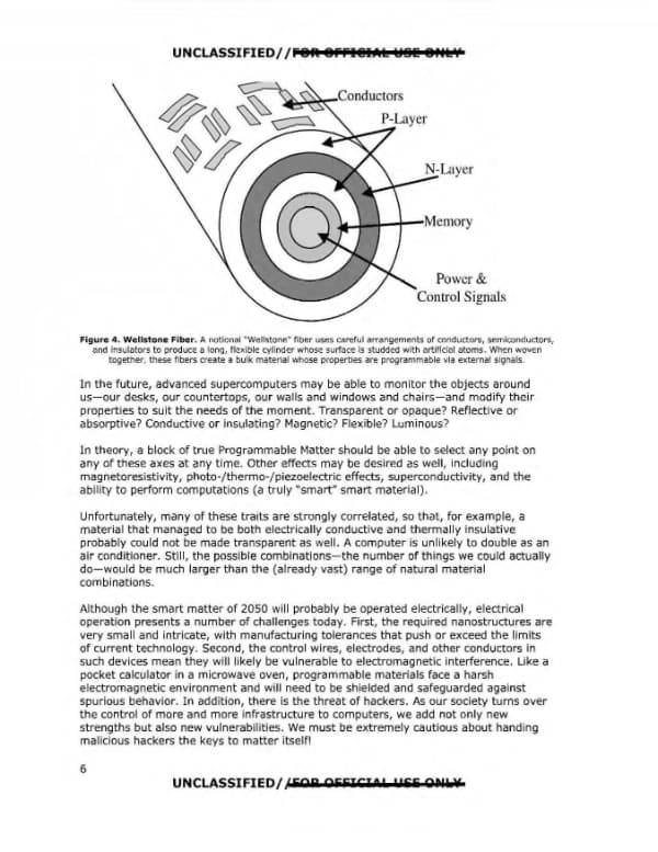
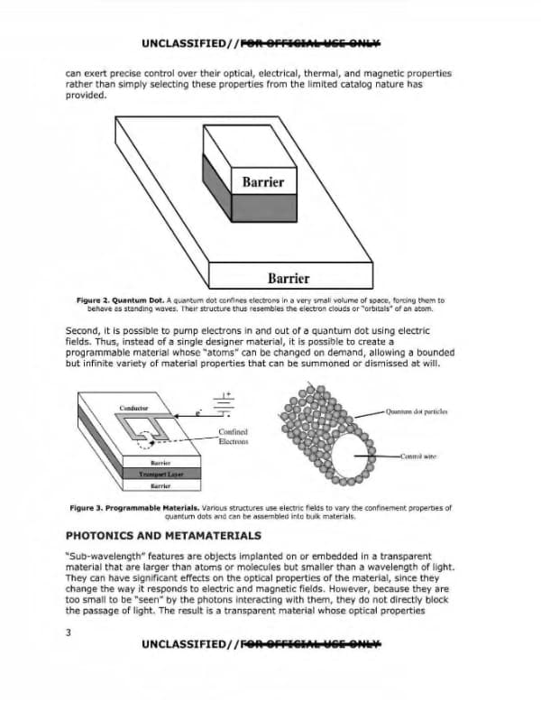
UNCLASSIFIED//FOR OFFICIAL USE ONLY Figure 4. Wellstone Fiber. A notional "Wellstone" fiber uses careful arrangements of conductors, semiconductors, and insulators to produce a long, flexible cylinder whose surface is studded with artificial atoms. When woven together, these fibers create a bulk material whose properties are programmable via external signals. In the future, advanced supercomputers may be able to monitor the objects around us-our desks, our countertops, our walls and windows and chairs-and modify their properties to suit the needs of the moment. Transparent or opaque? Reflective or absorptive? Conductive or insulating? Magnetic? Flexible? Luminous? In theory, a block of true Programmable Matter should be able to select any point on any of these axes at any time. Other effects may be desired as well, including magnetoresistivity, photo-/thermo-/piezoelectric effects, superconductivity, and the ability to perform computations (a truly "smart" smart material). Unfortunately, many of these traits are strongly correlated, so that, for example, a material that managed to be both electrically conductive and thermally insulative probably could not be made transparent as well. A computer is unlikely to double as an air conditioner. Still, the possible combinations-the number of things we could actually do-would be much larger than the (already vast) range of natural material combinations. Although the smart matter of 2050 will probably be operated electrically, electrical operation presents a number of challenges today. First, the required nanostructures are very small and intricate, with manufacturing tolerances that push or exceed the limits of current technology. Second, the control wires, electrodes, and other conductors in such devices mean they will likely be vulnerable to electromagnetic interference. Like a pocket calculator in a microwave oven, programmable materials face a harsh electromagnetic environment and will need to be shielded and safeguarded against spurious behavior. In addition, there is the threat of hackers. As our society turns over the control of more and more infrastructure to computers, we add not only new strengths but also new vulnerabilities. We must be extremely cautious about handing malicious hackers the keys to matter itself! 6 UNCLASSIFIED//FOR OFFICIAL USE ONLY
Page 11

Page 11 of 20

This is page 7 of a report on Programmable Matter smart materials, discussing temperature sensitivity, thermochromic materials, and a 2003 LBNL/ASHRAE study of dynamic windows and their energy savings. The page contains no redactions.

UNCLASSIFIED//FOR OFFICIAL USE ONLY The greatest challenge, however, is temperature. The resistance of an electrical wire varies with temperature, and while we scarcely notice the difference with the fat copper wiring in our houses, the delicate films and nanowires of Programmable Matter smart materials feel it very strongly. Other critical properties, such as the bandgaps of semiconductors, the optical spacing of photonic crystals, and the internal symmetries of liquid crystals, are also temperature sensitive and must be managed carefully to avoid overwhelming the control signals passing through the material. Early attempts at programmable quantum dot materials were so temperature sensitive that researchers found that altering temperature, rather than the electric field, was actually the easiest way to control the response of the materials. In fact, by selecting materials with higher temperature sensitivity, we were able to enhance these effects to produce thermally activated smart materials with no need for electric controls at all. Of course, materials that respond to temperature are not new. Thermochromic (color-changing) liquid-crystal thermometers are well known, and in the mid-1990s, Chinese researchers developed a thermochromic paint that turns a cool-blue shade when warm, a warm-red shade when cool, and pale green at room temperature. This was done mainly for thermal regulation-the paint allegedly could increase the temperature of a building by about 4°C in winter and decrease it by about s0 c in summer-although the researchers also claimed an aesthetic benefit to having a home's color match the season. Even more impressive effects could be achieved if black and white (or clear and silver) were available color choices. Although thermochromic building materials were very rare until recently, a number of other mechanisms-including electrochromics, photochromics, and automatic mechanical blinds-have been used to create "dynamic windows" that actively control solar heat gain in buildings and display many of the properties (if not the principles) of a true smart material. Buildings account for 40 percent of all energy consumed in the United States, including 71 percent of all electricity and 38 percent of all carbon dioxide emissions. Managing solar heat gain and controlling the building's thermal envelope are the most effective ways of reducing energy use. The same principles apply, of course, to spacecra~, for which solar heat is even more intense and nighttime (in the shadow of the Earth) is colder. In 2003, the U.S. Department of Energy's Lawrence Berkeley National Laboratory (LBNL), on behalf of the American Society of Heating, Refrigeration, and Air Conditioning Engineers (ASHRAE), performed a study focused on dynamic window systems capable of darkening or shading automatically such that the solar heat gain coefficient (SHGC) varied between 0.26 and 0.40. Analyses were performed for eight U.S. cities: Boston, Denver, Jacksonville, Kansas City, Phoenix, Sacramento, Seattle, and Washington, D.C. The ASHRAE study found that across all eight climate zones, buildings with low-emissivity ("low-E") glass saved an average of 8-15 percent on their total annual energy (heating, cooling, and ventilation) costs, whereas the addition of dynamic window systems saved an additional 6-19 percent. In other words, the savings associated with a dynamic window are approximately as large as the savings associated with low-E. Furthermore, because dynamic windows and low-E coatings save energy 7 UNCLASSIFIED//FOR OFFICIAL USE ONLY
Page 12

Page 12 of 20

A report page discussing the energy performance of dynamic windows compared with low-E glass, and the early commercialization of RavenBrick's RavenWindow smart film in 2009. It includes a figure showing RavenWindow and RavenLight filters in cold and hot states.

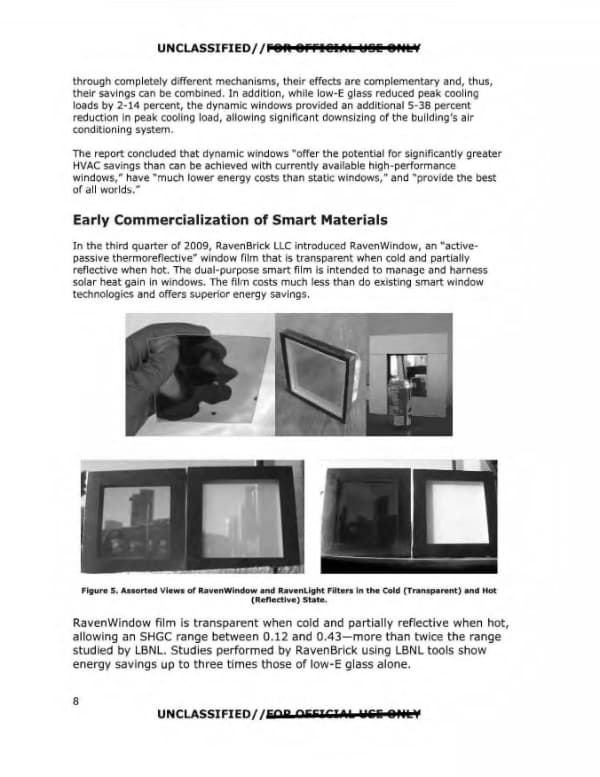
through completely different mechanisms, their effects are complementary and, thus, their savings can be combined. In addition, while low-E glass reduced peak cooling loads by 2-14 percent, the dynamic windows provided an additional 5-38 percent reduction in peak cooling load, allowing significant downsizing of the building's air conditioning system. The report concluded that dynamic windows "offer the potential for significantly greater HVAC savings than can be achieved with currently available high-performance windows," have "much lower energy costs than static windows," and "provide the best of all worlds." Early Commercialization of Smart Materials In the third quarter of 2009, RavenBrick LLC introduced RavenWindow, an "active-passive thermoreflective" window film that is transparent when cold and partially reflective when hot. The dual-purpose smart film is intended to manage and harness solar heat gain in windows. The film costs much less than do existing smart window technologies and offers superior energy savings. Figure 5. Assorted Views of RavenWindow and RavenLight Filters in the Cold (Transparent) and Hot (Reflective) State. RavenWindow film is transparent when cold and partially reflective when hot, allowing an SHGC range between 0.12 and 0.43\u2014more than twice the range studied by LBNL. Studies performed by RavenBrick using LBNL tools show energy savings up to three times those of low-E glass alone. 8